 EN
EN
 AR
AR
 CS
CS
 DA
DA
 NL
NL
 FI
FI
 FR
FR
 DE
DE
 EL
EL
 IT
IT
 JA
JA
 KO
KO
 NO
NO
 PL
PL
 PT
PT
 RO
RO
 RU
RU
 ES
ES
 TL
TL
 ID
ID
 SK
SK
 SL
SL
 UK
UK
 VI
VI
 TH
TH
 TR
TR
 AF
AF
 MS
MS
 SW
SW
 GA
GA
 CY
CY
 BE
BE
 KA
KA
 LO
LO
 LA
LA
 MI
MI
 MR
MR
 MN
MN
 NE
NE
 UZ
UZ

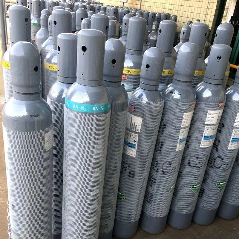
C3F8 gas, also called perfluoropropane, play an important role in microelectronics world. This gas get used in several processes that are essential for building small electronic components. You see these parts in everyday stuff like phones and laptops. At AGEM, we work on improving our products for customers, and knowing about gases like C3F8 help us better our making methods. Using C3F8 right can lead to higher quality and faster production of those tiny parts. This matter a lot in this quick-moving field.
What is C3F8 Gas and Its Role in Microelectronics?
C3F8 gas is a unique kind from the fluorinated gases group. It look colorless and odorless. In microelectronics, C3F8 take a key part in things like plasma etching. Plasma etching mean a method to make patterns on surfaces, which is vital for tiny circuits on silicon wafers. Those circuits form the base of microelectronics. When C3F8 gas get used in plasma etching, it remove unwanted stuff from the silicon surface. This step is needed for good electronic pieces. As C3F8 ionize, it make reactive bits that etch materials at small scales. So this allow fine details for modern tech gadgets. Using C3F8 also give cleaner surfaces. Manufacturers can keep fewer contamination on wafers with this gas. That’s why dirt or remains can mess up the final product work. In addition, C3F8 is a main tool for microelectronics makers. It help create better products, leading to reliable electronics for users. At AGEM, we see how important this gas is and try to use it for better production.
How C3F8 Gas Changes Plasma Etching Methods
C3F8 gas is really shaking up plasma etching ways. Old techniques usually had trouble with exactness and cleanness. But now, with C3F8 coming in, we can get super detailed results that match nothing else. The gas aid in making sharper etching patterns on silicon wafers. This is big because devices keep getting tinier and more tricky. As features shrink, need for precision rise, and C3F8 handle it well. One main plus of C3F8 is how it build a even etching space. This evenness let better control of the process, so fewer errors and higher quality overall. So makers can make devices that fit nice and run smoother. And C3F8 is kinder to the environment than some past gases. With this, companies like AGEM can cut their carbon mark while getting good production. Using C3F8 will also save money over time. Because it boost etching efficiency, makers save time and stuff. That mean more products quicker, which help everyone. To sum up, C3F8 transform etching methods to be more exact, quick, and green. At AGEM, we’re pumped about what C3F8 can do for microelectronics future.
Advantages of C3F8 in Semiconductor Making
C3F8, or perfluoropropane, is a special gas that bring lots of good things to semiconductor device production. The top benefit is how it make very exact and clean patterns on silicon wafers. These patterns matter as they help build small electronic bits that work smooth in things like smartphones. The clean patterns come from plasma etching, where C3F8 react with wafer materials. This let makers like AGEM produce chips that perform better and more efficient.
Another plus is C3F8 good at cutting down unwanted materials sticking to the wafer. In chip making, keeping clean from extra bits is key, or it can ruin things. C3F8 remove these extras, so products end up higher quality. That’s why chips with C3F8 usually last longer and work better, nice for device users.
In addition, C3F8 stand out for being more eco-friendly than other gases. Though gases affect the planet, C3F8 have lower warming potential. This help companies like AGEM who want to shrink their carbon footprint and care for earth. So by picking C3F8, AGEM give top semiconductor products and stay responsible. All this make C3F8 a solid pick for making semis, helping better and quicker electronics.
How to Make Plasma Etching Better with C3F8 Gas
To make plasma etching processes optimal with C3F8 gas, you need good planning and tweaking of factors for best outcomes. First, pick the right gear. Not every machine handle C3F8 the same, some suite it better. AGEM use advanced etching tools that work well with C3F8. So the gas can react right with wafer materials for exact and clean cuts.
Temperature in etching is another big thing. It can change how C3F8 perform. If too hot or cold, the gas might not do as wanted. AGEM watch and adjust temperature careful to keep it perfect. This get clean and right etching. Also, gas pressure tweak can improve results. Balancing pressure and temp is key to get most from C3F8 in etching.
Timing matter too. How long C3F8 apply affect etching quality. AGEM test different times to find the one that give precise results without harm to wafer. And keeping gear clean is must. Dirt in machines can mess C3F8 work. Regular clean and fix help process go smooth. By hitting these points, AGEM can improve etching, leading to superior semiconductor stuff.
How C3F8 Gas Boost Surface Treatment in Electronics
Surface treatment is a must step to ensure electronic devices run good. C3F8 gas make this step more efficient in a big way. When treating material surfaces with C3F8, it create smooth and clean finishes. This help because clean surface mean better sticking, so device parts join well. AGEM use C3F8 for surface treatment to make sure products have high quality and good performance.
C3F8 also cut down time for surface treatment. Old ways take long and less effective sometimes. But with C3F8, it go faster and better. So makers produce more devices quicker, good for customer needs. Plus, since C3F8 gas product remove unwanted stuff well, less need for extra cleaning after. This save time and resources.
One more gain is C3F8 improve device toughness. Proper treated surfaces make products less prone to damage. This nice for users wanting long-lasting electronics. AGEM aim to use C3F8 not just for efficient making but also for durable, reliable products. Overall, C3F8 make surface treatment quicker, cleaner, and stronger, which bring better devices to people.
Table of Contents
- C3F8 Gas in Microelectronics: Enhancing Plasma Etching and Surface Treatment Processes
- What is C3F8 Gas and Its Role in Microelectronics?
- How C3F8 Gas Changes Plasma Etching Methods
- Advantages of C3F8 in Semiconductor Making
- How to Make Plasma Etching Better with C3F8 Gas
- How C3F8 Gas Boost Surface Treatment in Electronics